Shreesha S
I am a 5th year Dual Degree student at Department of Electrical Engineering, Indian Institute of Technology Madras. As a part of my graduate thesis, I am working on a Pipelined Analog to Digital Converter (ADC) guided by Dr. Nagendra Krishnapura.
My research interests are Analog & Mixed Signal and Radio Frequency Integrated Circuits. This website gives an introduction of my research experience, and thank you for your time!
Education
Indian Institute Of Technology Madras
CGPA (upto 8th semester): 9.21
Minor: Mathematics For Computer Science
Important Coursework
Phase Locked Loops*
VLSI Broadband Communication Circuits
Analog IC Design
Analog Circuits
Electrical & Magnetic Circuits
Digital IC Design
Computer Architecture
Digital Systems
Introduction to Wireless & Cellular Communication
Computer (Communication) Networks
Digital Communication Systems
Device Modeling
Introduction to Photonics
Analog & Digital Filters
Mathematical Logic
Graph Theory
Theory Of Computation
Analog Circuits Laboratory
Advanced EE Laboratory
Microprocessor Laboratory
CAD Laboratory
*Not listed in transcript
Research Experience
A 10-bit 40-MSPS SAR ADC in TSMC65nm Process
This Successive Approximation Register (SAR) ADC is based on Monotonic Capacitor Switching Procedure. In the original paper a binary weighted 10-bit capacitor bank is used to acquire the signal.

In order to reduce the total capacitance, two capacitor banks are coupled as shown in Figure. However, this technique only generates approximate weights, and hence it may increase quantization noise.
While acquiring the signal, the top-plate of LSB bank can be connected to any voltage without affecting the resolved bits. Thus, this technique can be used to reduce input capacitance of SAR ADC, and thus has the potential to reduce the power consumption of the block driving the SAR ADC.
One of the cons of top plate sampling is the gain error caused by the parasitic capacitance at the top plate of MSB bank. To counter this, a layout technique is used, where signal is attenuated by the same factor as the capacitor weights. This technique however does not eliminate the gain error due to the gate capacitance of comparator and drain capacitor of sampling switches.

It can be shown that in the conventional structure (as shown in Fig.2) the digital logic delay is dependent on two flip flops. This can severely impact the settling-time requirements of switches connected to bottom plates of capacitors.
A new digital logic is designed to reduce logic delay, wherein the delay is dependent on only one flip flop instead of two.
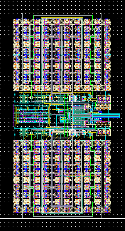
Fig.3 shows the layout of the fully differential ADC. This ADC design is currently in the process of fabrication.
Specifications of the ADC:
- Process: TSMC65nm
- Supply Voltage: 1.2 Volt
- Effective Number of Bits(ENOB): 9.5
- Power Consumption: 411uW
- Figure Of Merit (FOM) (lower is better): 13.65 fJ/conversion
- Area consumed: 300uM * 150uM
Front end 4-bit MSB stage for a 16-bit 5-MSPS Pipelined ADC in UMC180nm process

I am designing a gain boosted folded cascode amplifier for the first stage of pipelined adc. The OTA of pipelined adc needs to have a clean 20 dB/dec roll-off to get a good settling behaviour. A folded cascode has a gain corresponding to two stages, reasonable voltage swing limits and a single pole frequency response. Gain boosting technique can increase the DC gain of the amplifier without any trade-offs with the bandwidth of the amplifier. Also it can be shown that the bandwidth of gain boosting amplifier does not need to be as high as the bandwidth of the main amplifier, so this technique can be implemented without spending too much power. I was able to achieve 115 dB DC gain with a unity gain bandwidth of 280 MHz while driving a 9pF load capacitor. Furthermore, new techniques are being developed to reduce the power consumption of OTA, and it is expected to reduce power consumption by about 30%.
Internship at Texas Instruments, Bengaluru
I have drafted a resistive DAC element for SD ADC in 28nm process, operating at a clock frequency of 1.5 GHz and supply voltage of 1 volt. The DAC was made up of resistors being driven by inverters. One of the problems I faced was reducing rise-fall time mismatch. In differential systems inherently there is no rise-fall time mismatch, however because of random mismatch between PMOS transistors (and NMOS) of two arms of the differential circuit, there can be a finite rise-fall time mismatch. This becomes challenging when optimizing for power, since sizes of transistors needs to be reduced. Two designs were proposed:
- The first circuit attempts to match rise and fall time of a single arm. Even though PMOS primarily impacts rise-time (and NMOS fall-time) a transmission gate allows both transistors to control both rise & fall times.
- The second circuit attempts to match rise-times of differential arms by making the rise-times dependent on a single common transistor (and similarly for the fall-times as well). This seems to be a more general solution.
Other Projects
IITMSAT
IITMSAT is a student satellite project to build a satellite which is aimed at studying the features of plasma in the upper ionosphere and characterize its relation with earth-based phenomena like seismic activity. The satellite is undergoing Qualification Model (QM) tests.
- Involved in the development of on-board communication software. The project included designing a robust telecommand and telemetry manager, delegating various tasks to subsystem routines like payload data receiver, beacon, on-board data storage, encoder and decoder for communication with ground station
- Implemented algorithms like convolution-encoding, cyclic-redundancy-check, bit-de-stuffing, direct-memory-access to receive serial data
- Tracked and logged satellites like SRM-SAT etc. with the help of Perseus Radio.
- Involved in ground station rotor and antenna setup
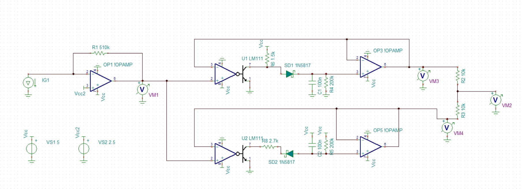
0.75-1.5 GHz wideband Phase Locked Loop in UMC180nm Technology
This was a course project to design an integer-N wideband 0.75-1.5 GHz PLL operating with a reference frequency of 46.875 MHz. The required specifications were, -40 dBc reference spur, -10 dB worst case PHI_OUT/Vsupply (Power Supply Noise Rejection), <1% absolute jitter. Following schematics show some of the components.

To maintain good matching between I_UP and I_DN throughout all possible values of Vctrl (of VCO), PMOS bias is generated based on the loop-filter capacitor voltage (Vc). This arrangement is shown in Fig.1.

To avoid peaking of PHI_OUT/Vsupply, a regulator with replica load has been used. The bandwidth of regulator has to be higher than PLL bandwidth. Regulator will reject in-band supply noise, and the second pole of VCO and its current source reject out-of band supply noise.
In Fig.2 the inverter sizes and capacitors are adjusted such that the current consumed is about 4 times lesser than VCO. To keep the VCO current source in saturation, the current consumed in replica must be slightly lesser than 4 times.
5 Gbps Wireline Link in 45nm process
As part of VLSI Broadband Communication Circuits course I have drafted a 5 Gbps serial link in 45nm process connected through a channel with 15dB channel loss at 2.5 GHz.
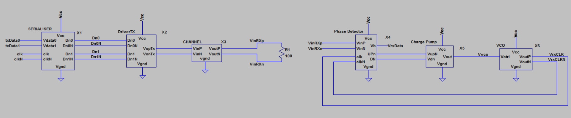
The transmitter is made up of a 2:1 serialiser that takes in two data streams at 2.5 Gbps and outputs a single stream at 5 Gbps datarate. This data is passed through a voltage mode equalizer which drives the channel and offers 50 ohm output impedance. In this design most of the power is consumed in this equalizer.
At the receiver, the data is sampled through a strong arm latch since the voltage swings are not high enough to directly operate a flip flop. The clock of the VCO is locked such that the rising edge of the clock occurs at the middle of the bit-period.
LiFi Project at CFI
This was a project to build a working LiFi model under Electronics Club, CFI, IIT Madras. I was able to achieve 200 kbps at close range while using LF347 as a trans-impedance amplifier. This was presented at CFI Open House in November 2016.
Skills
- C/C++
- Python
- Verilog
- MATLAB
- Cadence Virtuoso
- Innovus/Genus (Digital Synthesis Tools)
- MATLAB
- LTSpice
- MBED Platform
Scholastic Achievements
- Ranked among the top ten in the 2018 batch of Dual-Degree Electrical Engineering at IIT Madras
- Secured an All India Rank of 1055 in Joint-Entrance-Exam (JEE) Advanced 2013
- Scored 93% marks in Class XII, Department of Pre-University Education, Karnataka in 2013
- Scored 97% marks in Class X, Karnataka Secondary Education Examination Board in 2011